In our last article, we covered some of the techniques that are being used to create printed circuit boards using a 3D printer. Following those, you should have the copper traces you need for your board layout. It may look neat, but the board won’t do a whole lot without any components on it. Now we need to add the magic…the resistors, chips, capacitors, and other electronics that really make things go.
A precautionary note: as with last article, this is just an overview. Make sure you look further into the methods used, and take necessary precautions.
Picking and Placing
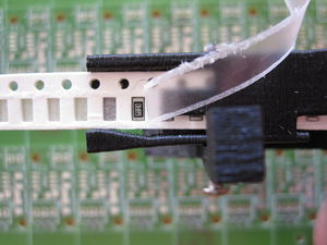
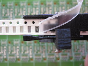
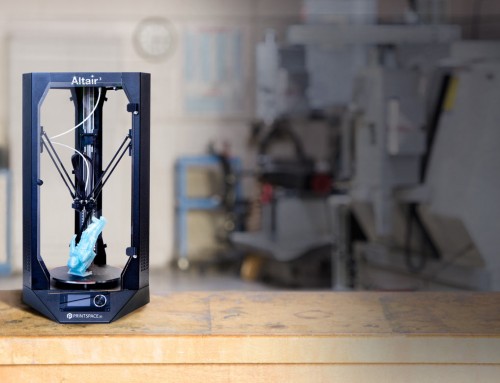
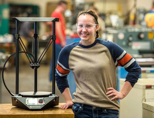
The next steps in the process can be broken down into placing the components, then soldering them on to the PCB. Placing the components on the board are typically done using a pick and place machine, designed to pick up the components and put them in the correct location on the PCB. Consumer models (which follow a delta printer design similar to the Altair) are beginning to filter into the market.
Electronics, Lightly Toasted
Soldering the components in place tends to be done using solder paste at this point. The solder paste can be applied using a custom extruder tool head, then the board is heated. The heating bakes the paste, making it solid and forming the board contacts to the traces.
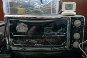
One convenient way of heating the board has been using an old toaster oven, believe it or not. The temperature control allows you to dial it in to the correct temperature, about 200 degrees Fahrenheit. The biggest concern is frying the chips – too warm and it can damage components and too cool and the solder won’t flow correctly. Regardless this will probably involve some trial and error the first few times.
After the paste has been heated, the board can cool and any clean up of the board can be done. This includes trimming long leads off components and touch up of potential problems with a soldering iron.
After clean up, the board should be done. People have been making their own PCBs for a while, but a workflow using the advantages of 3D printing is still pretty new. You’re not going to find model repositories devoted to etching masks quite yet, or pre-designed pick and place instruction repos. But it is still very cool, and we can expect to see more about this in the future.
